cara mengobati herpes di selangkangan - Penyakit herpes genital baik pada pria maupun pada wanita kerap menjadi permasalahan tersendiri, karena resiko yang lebih besar dibanding penyakit herpes pada umumnya, penyakit herpes genital juga kerap menjadi aib bai penderitanya dikarena jenis penyakit herpes genital disebabkan sebagian besar dikarenakan seks bebas.
cara mengobati herpes di selangkangan - Pertanyaan yang sering diajukan adalah apakah jenis virusnya sama dengan penyakit herpes yang lain? dan apakah harus dengan obat tertentu untuk mengobati penyakit herpes genital

Herpes adalah penyakit menular seksual (PMS) yang disebabkan oleh virus herpes simpleks (HSV). Ada dua jenis HSV,ya itu Herpes Simplex 1 (HSV1) dan Herpes Simplex 2 (HSV-2). HSV1 atau herpes di mulut umumnya ditemukan dalam bentuk luka dingin di sekitar mulut . HSV-2 atau Herpes kelamin adalah bentuk herpes yang jauh lebih intens, yang umumnya ditemukan pada alat kelamin. Namun KEDUA jenis HSV ini dapat ditemukan di mulut atau daerah kelamin. Seseorang mungkin terinfeksi dengan HSV-1 dan HSV-2. Terinfeksi oleh satu dari tersebut tidak membuat Anda kebal terhadap yang lain.
GEJALA PENYAKIT HERPES
Penyakit herpes merupakan penyakit yang meradang pada kulit dan biasanya muncul gelembung yang berisi air dan berkelompok. Penyakit Herpes terdiri dari dua macam yaitu herpes zoster, penyakit herpes yang menyerang kulit. Dan herpes genitalis adalah penyakit herpes yang merupakan salah satu penyakit kelamin. Ciri-ciri herpes ini yaitu rasa sesak nafas, demam, mengigil, sendi terasa nyari, pegal hanya pada satu bagian tubuh sajaobat herpes genital pada pria
Pada herpes simplex mulut dan bibir, gambaran gejalanya sangat khas. Pada bibir akan tumbuh lenting – lenting bening seukuran kepala jarum pentul dan sifatnya bergerombol. Lenting ini tumbuhnya terdapat pada perbatasan selaput merah bibir dengan kulit dan akan tampak agak kemerahan. Bila herpes mulai menyerang, akan disertai dengan rasa tidak enak badan, demam, serta nyeri kepala.

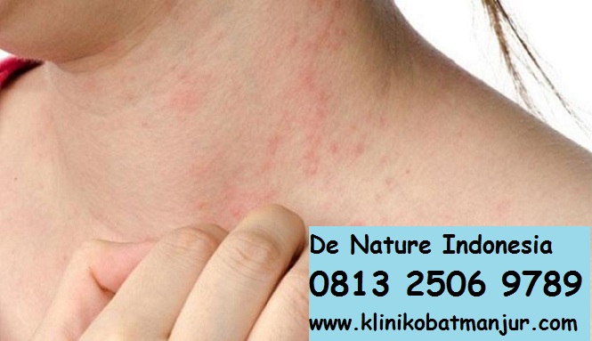
Sedangkan gejala herpes genital yang paling umum adalah sekelompok luka blister pada vagina, vulva, leher rahim, penis, pantat, atau anus. Gejala dapat berlangsung beberapa minggu dan pergi. Mereka mungkin kembali dalam minggu, bulan, atau tahun. Saat pertama gejala herpes genital muncul disebut “episode pertama” atau “herpes awal.” Herpes awal gejala biasanya lebih terlihat dibandingkan episode berikutnya.
- Lecet
- Perasaan terbakar jika air seni mengalir di atas luka
- Ketidakmampuan untuk buang air kecil jika pembengkakan luka yang parah memblokir uretra
- Gatal
- Luka terbuka
- Nyeri pada daerah yang terinfeksi
Penularan Herpes
Seluruh jenis penyakit herpes dapat menular melalui kontak langsung. Namun pada herpes zoster, seperti yang terjadi pada penyakit cacar (chickenpox), proses penularan bisa melalui bersin, batuk, pakaian yang tercemar dan sentuhan ke atas gelembung/lepuh yang pecah. Pada penyakit Herpes Genitalis (genetalia), penularan terjadi melalui prilaku sex. Sehingga penyakit Herpes genetalis ini kadang diderita dibagian mulut akibat oral sex.

Seseorang yang pernah mengalami cacar air dan kemudian sembuh, sebenarnya virus tidak 100% hilang dari dalam tubuhnya, melainkan bersembunyi di dalam sel ganglion dorsalis sistem saraf sensoris penderita. Ketika daya tahan tubuh (Immun) melemah, virus akan kembali menyerang dalam bentuk Herpes zoster dimana gejala yang ditimbulkan sama dengan penyakit cacar air (chickenpox). Bagi seseorang yang belum pernah mengalami cacar air, apabila terserang virus varicella-zoster maka tidak langsung mengalami penyakit herpes zoster akan tetapi mengalami cacar air terlebih dahulu.
Pencegahan Herpes
- Berhenti melakukan hubungan seksual segera setelah Anda merasakan tanda-tanda awal infeksi. Tanda-tanda awal infeksi mungkin termasuk rasa terbakar, gatal, atau kesemutan. Jangan berhubungan seks vaginal, anal, atau oral, bahkan dengan kondom. Tunggu sampai tujuh hari setelah sembuh. Virus ini dapat menyebar dari luka yang tidak tertutup oleh kondom. Virus juga dapat menyebar lewat cairan keringat atau vagina ke tempat yang tidak tertutup kondom.
- Gunakan kondom di antara episode gejala untuk mengurangi risiko penularan.
- Gunakan pengobatan herpes. Risiko penularan dapat sangat dikurangi jika pasangan penderita herpes mengambil dosis kecil obat anti-herpes.
Pengobatan Penyakit Herpes Dengan Cara Herbal Paling Efektif
Pengobatan penyakit herpes dengan cara pengobatan secara herbal dengan menggunakan obat herpes dari De Nature yang sudah teruji khasiatnya untuk mengobati penyakit herpes, bahkan kegunaanya untuk menyembuhkan berbagai macam penyakit kulit lainnya, bahkan yang sudah membandel sekalipun.

Untuk Sobat yang sedang mencari pengobatan penyakit herpes yang ampuh, alhamdulilah kami De Nature Menyediakan obat herbal khusus untuk herpes yang sangat ampuh atasi penyakit ini. Penyakit herpes saat ini bisa disembuhkan melalui metode pengobatan tradisional. Seperti yang dilakukan oleh kami, yang sudah lama menyembuhkan para penderita penyakit herpes.
KELEBIHAN BELANJA ONLINE PADA KAMI (DE NATURE INDONESIA)
- Setiap penyakit berbeda obatnya, jd obat kami khusus untuk penyakit itu sendiri!
- Harga lebih murah
- Kualitas terbaik
- Tanpa perlu pergi ke dokter (tidak malu saat ke dokter, hemat waktu, dll)
- Tidak perlu disuntik
- Masa penyembuhannya singkat Proses obat hanya 2 – 3 hari
- Barang dikirim ke alamat rumah Anda via TIKI, JNE kilat, dibungkus rapi. Dan RAHASIA DIJAMIN.
- Proses pengiriman cepat dan aman
- Botol obat sengaja kami buat polos agar tidak ada yang tahu isinya apa, privasi Anda lebih terjamin.
- Hanya kami yang selalu mengutamakan ke puasan konsumen
Untuk Informadsi Dan Pemesanan